- 您现在的位置:买卖IC网 > Sheet目录338 > LT3754IUH#TRPBF (Linear Technology)IC LED DVR 16CH 50MA 32QFN
�� �
�
�LT3754�
�BLOCK� DIAGRAM�
�13�
�SHDN� /UVLO�
�+�
�12�
�V� IN�
�11�
�INTV� CC�
�7V(REGULATED)�
�UVLO(� +� )� =� 3.8V,� UVLO(� ?� )� =� 3.4V�
�600k�
�1.476V�
�–�
�–� +�
�V� C�
�–� +�
�SLOPE�
�OSC�
�R�
�S�
�Q�
�EN�
�GATE�
�SYNC�
�RT�
�10�
�15�
�25�
�SENSE�
�V� OUT�
�27�
�31�
�REF�
�1.485V�
�PWM�
�V� REF�
�+�
�–�
�INTV� CC_UV�
�V� IN_UV�
�SHDN_UV�
�4.2V(� +� )�
�3.7V(� ?� )�
�1.485V�
�EN�
�+�
�–�
�EN�
�6V�
�LED�
�LOGIC�
�52mV�
�PEAK�
�CURRENT�
�SOFT�
�START�
�100mV�
�OVER�
�CURRENT�
�HICCUP__MODE�
�LEDx�
�1-8,� 17-24�
�FAULT�
�EN�
�9�
�16�
�14�
�+�
�–�
�29�
�CTRL�
�1V�
�+�
�+�
�LED� CURRENT�
�CONTROL�
�CHANNEL� X�
�1.1V�
�LED� AMP�
�SS�
�OVERVOLTAGE�
�AMP�
�PWM�
�56R�
�–� +�
�R�
�V� PTAT�
�30�
�T� SET�
�32�
�I� SET�
�33�
�EXPOSED� PAD� (GND)�
�26�
�V� C�
�28�
�OVP� SET�
�3754� BD�
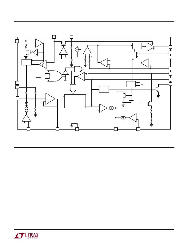
�Figure� 1.� LT3754� Block� Diagram�
�OPERATION�
�The� operation� of� the� LT3754� is� best� understood� by� referring�
�to� the� typical� application� circuit� on� the� front� page� and� the�
�Block� Diagram� in� Figure� 1.� The� LT3754� drives� 16� strings�
�of� LEDs� by� using� a� constant� switching� frequency,� current�
�mode� boost� controller� to� generate� a� single� output� voltage�
�V� OUT� for� the� top� (anode)� of� all� LED� strings.� LED� string�
�current� is� generated� and� controlled� by� connection� of� the�
�bottom� LED� in� each� string� (cathode)� to� a� current� source�
�contained� in� each� corresponding� LED� pin.� Each� LED� pin�
�contains� an� accurate� current� sink� to� ground,� programmable�
�between� 10mA� to� 50mA� using� a� single� resistor� at� the� I� SET�
�pin.� LED� channels� can� be� paralleled� to� achieve� higher� LED�
�currents.� For� applications� requiring� less� than� 16� strings�
�of� LEDs,� channels� can� be� paralleled� or� disabled� (connect�
�LED� pin� to� V� OUT� before� start-up).� For� optimum� efficiency,�
�V� OUT� regulates� to� the� lowest� possible� voltage� allowable� to�
�maintain� regulated� current� in� each� LED� string.� Any� OPEN�
�LED� fault� is� indicated� by� the� FAULT� pin� driven� low� without�
�effecting� the� operation� of� the� connected� LED� strings.�
�The� Block� Diagram� in� Figure� 1� illustrates� the� key� functions�
�of� the� LT3754.� It� can� be� seen� that� two� external� supplies,�
�V� REF� and� INTV� CC� ,� are� generated� by� the� LT3754.� The� V� REF�
�pin� provides� a� precision� 1.485V� output� for� use� with� external�
�resistors� to� program� the� CTRL,� OVP� SET� and� T� SET� input�
�pins.� The� INTV� CC� pin� provides� a� regulated� 7V� output� to�
�supply� the� gate� driver� for� the� boost� controller� GATE� pin.�
�An� accurate� 1.476V� threshold� on� the� SHDN� /UVLO� pin�
�combined� with� a� SHDN� /UVLO� pin� current� hysteresis� allows�
�a� programmable� resistor� divider� from� V� IN� to� SHDN� /UVLO�
�3754fc�
�9�
�发布紧急采购,3分钟左右您将得到回复。
相关PDF资料
LT3755EMSE#PBF
IC LED DRVR HP CONS CURR 16-MSOP
LT3760EFE#PBF
IC LED DVR WHT/CLR BCKLT 28TSSOP
LT3799IMSE#PBF
IC LED DRIVER TRIAC DIM 16-MSOP
LT3956EUHE#PBF
IC LED DVR BUCK BOOST 36-VQFN
LTC3201EMS#TRPBF
IC LED DRVR WHITE BCKLGT 10-MSOP
LTC3202EDD#PBF
IC LED DRIVR WHITE BCKLGT 10-DFN
LTC3205EUF#TRPBF
IC LED DRVR WT/RGB BCKLGT 24-QFN
LTC3206EUF#TRPBF
IC LED DRVR WT/RGB BCKLGT 24-QFN
相关代理商/技术参数
LT3754IUHPBF
制造商:LINER 制造商全称:Linear Technology 功能描述:16-Channel × 50mA LED Driver
LT3754IUHTRPBF
制造商:LINER 制造商全称:Linear Technology 功能描述:16-Channel × 50mA LED Driver
LT3755
制造商:LINER 制造商全称:Linear Technology 功能描述:60V 4-Switch Synchronous
LT3755-1
制造商:LINER 制造商全称:Linear Technology 功能描述:60V 4-Switch Synchronous
LT3755-2
制造商:LINER 制造商全称:Linear Technology 功能描述:60V 4-Switch Synchronous
LT3755EMSE#PBF
功能描述:IC LED DRVR HP CONS CURR 16-MSOP RoHS:是 类别:集成电路 (IC) >> PMIC - LED 驱动器 系列:- 标准包装:60 系列:- 恒定电流:- 恒定电压:- 拓扑:线性(LDO),PWM,升压(升压) 输出数:8 内部驱动器:是 类型 - 主要:背光 类型 - 次要:RGB,白色 LED 频率:500kHz ~ 1.5MHz 电源电压:4.75 V ~ 26 V 输出电压:45V 安装类型:* 封装/外壳:* 供应商设备封装:* 包装:* 工作温度:-40°C ~ 85°C
LT3755EMSE#PBF
制造商:Linear Technology 功能描述:DRIVER LED 40VIN 1MHZ 16MSOP 制造商:Linear Technology 功能描述:DRIVER, LED, 40VIN, 1MHZ, 16MSOP
LT3755EMSE#TRPBF
功能描述:IC LED DRVR HP CONS CURR 16-MSOP RoHS:是 类别:集成电路 (IC) >> PMIC - LED 驱动器 系列:- 标准包装:6,000 系列:- 恒定电流:- 恒定电压:- 拓扑:开路漏极,PWM 输出数:4 内部驱动器:是 类型 - 主要:LED 闪烁器 类型 - 次要:- 频率:400kHz 电源电压:2.3 V ~ 5.5 V 输出电压:- 安装类型:表面贴装 封装/外壳:8-VFDFN 裸露焊盘 供应商设备封装:8-HVSON 包装:带卷 (TR) 工作温度:-40°C ~ 85°C 其它名称:935286881118PCA9553TK/02-TPCA9553TK/02-T-ND